According to media reports, the Suwon District Court in South Korea recently sentenced a former researcher at SEMES to four years in prison for illegally obtaining patent technology related to the company’s semiconductor cleaning equipment and using this technology to manufacture similar tools for export to China.
In the semiconductor industry, high-purity (electronic-grade) carbon dioxide is mainly used for cleaning technology and immersion lithography. With the increasing number of cleaning procedures in Fab factories, the demand for high-purity (electronic-grade) carbon dioxide in China will also increase in the future. Chip cleaning used to be simply immersing the chip in a cleaning solution. However, from FinFET to GAA structure, advanced DRAM and 3D-NAND, cleaning technology has entered the third stage and is now becoming one of the main challenges in semiconductor advanced processes. What role does high-purity (electronic-grade) carbon dioxide play in semiconductor manufacturing?
1.High purity carbon dioxide is used for cleaning high aspect ratio trenches and micro-holes
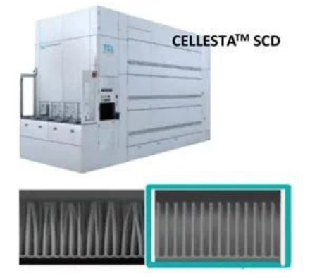
Supercritical carbon dioxide cleaning technology is used for cleaning high aspect ratio trenches and micro-holes in semiconductor integrated circuits. The cleaning process involves using pulses of supercritical carbon dioxide, which involves periodically changing the pressure near the critical point of carbon dioxide, causing it to oscillate between the supercritical and subcritical regions. The small pressure changes near the critical point of carbon dioxide can result in significant changes in density, which are utilized to remove particles from the trenches and micro-holes.
Supercritical cleaning uses supercritical carbon dioxide to clean semiconductor devices. This technology is the next generation technology that can minimize damage. An expert in the gas field once participated in the design of a high-pressure vessel for supercritical carbon dioxide cleaning of semiconductor equipment in China. According to the currently available patents for supercritical fluid semiconductor cleaning technology using carbon dioxide, the existing technology in China mainly focuses on effectively cleaning the microstructures on the surface of the silicon wafer, and rarely involves cleaning technology for the microstructures of semiconductor devices. TEL from Japan has shared information on semiconductor supercritical equipment and pattern collapse prevention drying technology in public speeches.
2. High-purity carbon dioxide is used for immersion lithography
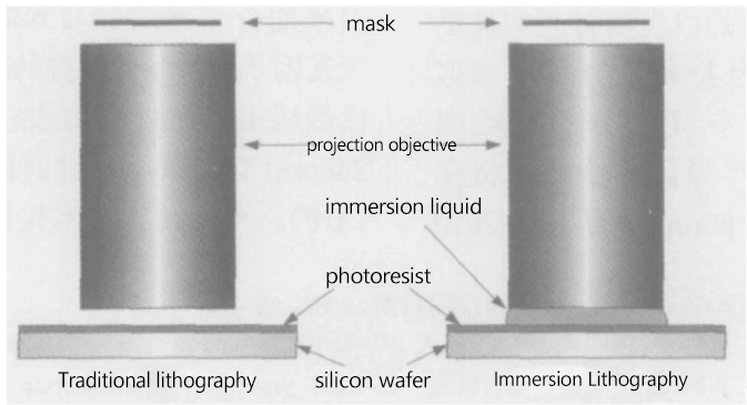
Immersion lithography, also known as immersion-based lithography, generally refers to 193nm immersion lithography. By filling the space between the final lens on the projection lens of the lithography machine and the photoresist on the silicon wafer with a high refractive index liquid (such as deionized water), the lithography resolution is further improved and the wavelength bottleneck of the light source is broken. After further purification, degassing, and temperature control, the deionized water flows into the exposure head, fills the space between the wafer and the lens, and then flows out of the lithography machine. High-purity carbon dioxide is used to prevent the liquid from leaking out from the side.
3. High-purity carbon dioxide is used for third-generation semiconductors
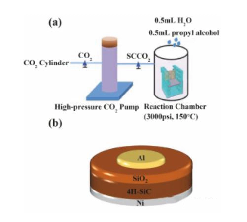
The interface quality between silicon carbide and silicon dioxide can limit the performance of silicon carbide field-effect transistors. Researchersfrom Xi’an Jiaotong University and Xidian University in China say this deficiency can be addressed through supercritical carbon dioxide processing, which can reduce the interface state density. The team’s spokesperson told”Compound Semiconductor” that in traditional silicon carbide field-effect transistors, the interface cannot be optimized through high-temperature annealing, as this would produce carbon clusters and other defects. Supercritical carbon dioxide treatment at lower temperatures can eliminate the formation of these defects, ensuring higher carrier mobility, lower leakage current, and an increased critical breakdown field for the gate oxide.


